 | –≠–ª–µ–∫—Ç—Ä–æ–Ω–Ω—ã–π –∫–æ–º–ø–æ–Ω–µ–Ω—Ç: SP2526 | –°–∫–∞—á–∞—Ç—å:  PDF PDF  ZIP ZIP |

1
Rev. 8/21/01 SP2526 +3.0V to +5.5V USB Power Control Switch © Copyright 2001 Sipex Corporation
s
Compliant to USB Specifications
s
+3.0V to +5.5V Input Voltage Range
s
Two Independent Power Switches
s
Two Error Flag Outputs, Open Drain
s
2.7V Undervoltage Lockout
s
500mA Minimum Continuous Load
Current Per Switch
s
1.25A Short Circuit Current Limit
s
140m
Maximum On-Resistance
SP2526
DESCRIPTION
The SP2526 device is a dual +3.0V to +5.5V USB Supervisory Power Control Switch ideal for
self-powered and bus-powered Universal Serial Bus (USB) applications. Each switch has low
on-resistance (80m
typical) and can supply 500mA minimum. The fault currents are limited
to 2.0A typical and the flag output pin for each switch is available to indicate fault conditions
to the USB controller. The 1ms soft start will eliminate any momentary voltage droop on the
upstream port that may occur when the switch is enabled in bus-powered applications. The
thermal shutdown feature will prevent damage to the device when subjected to excessive
current loads. The undervoltage lockout feature will ensure that the device will remain off
unless there is a valid input voltage present.
ENA
GND
OUTA
FLGA
FLGB
OUTB
IN
ENB
SP2526
8
7
4
3
2
1
5
6
+3.0V to +5.5V USB Power Control Switch
Æ
s
80
µ
A On-State Supply Current
s
1
µ
A Shutdown Current
s
Output Can Be Forced Higher Than
Input (Off-State)
s
Thermal Shutdown
s
1ms Soft-Start Power Up
s
Active-High Version: SP2526-1
s
Active-Low Version: SP2526-2
2
Rev. 8/21/01 SP2526 +3.0V to +5.5V USB Power Control Switch © Copyright 2001 Sipex Corporation
ABSOLUTE MAXIMUM RATINGS
These are stress ratings only and functional operation
of the device at these ratings or any other above those
indicated in the operation sections of the specifica-
tions below is not implied. Exposure to absolute maxi-
mum rating conditions for extended periods of time
may affect reliability.
Supply Voltage......................................-0.3V, +6.0V
Operating Temperature.....................-40∞C to +85∞C
Storage Temperature......................-65∞C to +150∞C
Power Dissipation Per Package
8-pin NSOIC
(derate 6.14mW/
O
C above+70
O
C).................500mW
8-pin PDIP
(derate 11.8mW/
O
C above+70
O
C)...............1000mW
SPECIFICATIONS
Unless otherwise noted, the following specifications apply for V
IN
= +5.0V, T
A
= 25
∞
C.
R
E
T
E
M
A
R
A
P
.
N
I
M
.
P
Y
T
.
X
A
M
S
T
I
N
U
S
N
O
I
T
I
D
N
O
C
V
,
e
g
n
a
R
e
g
a
t
l
o
V
g
n
i
t
a
r
e
p
O
N
I
0
.
3
5
.
5
V
I
,
t
n
e
r
r
u
C
y
l
p
p
u
S
N
I
5
0
.
0
0
8
0
.
5
0
6
1
µ
A
d
a
o
l
t
u
p
t
u
o
o
n
,
f
f
o
e
l
b
a
n
e
d
a
o
l
t
u
p
t
u
o
o
n
,
n
o
e
l
b
a
n
e
d
l
o
h
s
e
r
h
T
t
u
p
n
I
e
l
b
a
n
E
e
g
a
t
l
o
V
8
.
0
1
.
2
9
.
1
4
.
2
V
n
o
i
t
i
s
n
a
r
t
h
g
i
h
o
t
w
o
l
n
o
i
t
i
s
n
a
r
t
w
o
l
o
t
h
g
i
h
t
n
e
r
r
u
C
t
u
p
n
I
e
l
b
a
n
E
1
0
.
0
1
0
.
0
1
1
µ
A
V
N
E
V
=
)
n
i
m
(
H
O
V
4
.
2
=
V
N
E
V
=
)
x
a
m
(
L
O
V
8
.
0
=
e
c
n
a
t
i
c
a
p
a
C
t
u
p
n
I
e
l
b
a
n
E
1
F
p
e
c
n
a
t
s
i
s
e
R
h
c
t
i
w
S
0
8
0
4
1
m
V
3
.
3
<V
N
I
<
I
,
V
0
.
5
L
<
A
m
0
0
5
y
a
l
e
D
n
O
-
n
r
u
T
t
u
p
t
u
O
5
.
0
s
m
R
L
0
1
=
t
u
p
t
u
o
h
c
a
e
e
m
i
T
e
s
i
R
n
O
-
n
r
u
T
t
u
p
t
u
O
1
s
m
R
L
0
1
=
t
u
p
t
u
o
h
c
a
e
y
a
l
e
D
f
f
O
-
n
r
u
T
t
u
p
t
u
O
1
0
2
µ
s
R
L
0
1
=
t
u
p
t
u
o
h
c
a
e
e
m
i
T
ll
a
F
f
f
O
-
n
r
u
T
t
u
p
t
u
O
1
0
2
µ
s
R
L
0
1
=
t
u
p
t
u
o
h
c
a
e
t
n
e
r
r
u
C
e
g
a
k
a
e
L
t
u
p
t
u
O
2
0
.
0
1
µ
A
t
u
p
t
u
o
h
c
a
e
d
l
o
h
s
e
r
h
T
t
i
m
i
L
t
n
e
r
r
u
C
0
.
2
8
.
2
A
t
u
p
t
u
o
e
l
b
a
n
e
o
t
d
e
il
p
p
a
d
a
o
l
d
e
p
m
a
R
,
t
u
p
t
u
o
h
c
a
e
t
i
m
i
L
t
n
e
r
r
u
C
t
i
u
c
r
i
C
-
t
r
o
h
S
5
.
0
5
7
.
0
5
2
.
1
A
V
,
t
u
p
t
u
o
h
c
a
e
T
U
O
V
0
=
n
w
o
d
t
u
h
S
e
r
u
t
a
r
e
p
m
e
T
-
r
e
v
O
d
l
o
h
s
e
r
h
T
5
3
1
5
2
1
O
C
e
r
u
t
a
r
e
p
m
e
t
g
n
i
s
a
e
r
c
n
i
e
r
u
t
a
r
e
p
m
e
t
g
n
i
s
a
e
r
c
e
d
e
c
n
a
t
s
i
s
e
R
t
u
p
t
u
O
g
a
l
F
r
o
r
r
E
0
1
5
1
5
2
0
4
V
N
I
I
,
V
5
=
L
A
m
0
1
=
V
N
I
I
,
V
3
.
3
=
L
A
m
0
1
=
t
n
e
r
r
u
C
f
f
O
g
a
l
F
r
o
r
r
E
1
0
.
0
1
µ
A
V
G
A
L
F
V
5
=
d
l
o
h
s
e
r
h
T
O
L
V
U
5
.
2
7
.
2
6
.
2
0
.
3
V
V
N
I
T
,
g
n
i
s
a
e
r
c
n
i
N
I
M
T
o
t
X
A
M
,
V
N
I
g
n
i
s
a
e
r
c
e
d
,
T
N
I
M
T
o
t
X
A
M
3
Rev. 8/21/01 SP2526 +3.0V to +5.5V USB Power Control Switch © Copyright 2001 Sipex Corporation
PIN ASSIGNMENTS
Pin 1 -- ENA -- Enable Input for MOSFET
Switch A. This input pin is active high for the
SP2526-1 and active low for the SP2526-2.
Pin 2 -- FLGA -- Fault Flag Output for Switch
Channel A. This open drain output pin pulls
low to indicate overcurrent, undervoltage
lockout, and thermal shutdown conditions.
Pin 3 -- FLGB -- Fault Flag Output for Switch
Channel B. This open drain output pin pulls
low to indicate overcurrent, undervoltage
lockout, and thermal shutdown conditions.
Pin 4 -- ENB -- Enable Input for MOSFET
Switch B. This input pin is active high for the
SP2526-1 and active low for the SP2526-2.
.
Pin 5 -- OUTA -- Output for MOSFET Switch
Channel A. This is the output pin of the
MOSFET source of channel A, typically
connected to the switched side of the load.
Pin 6 -- GND -- Ground reference. Supply
return.
Pin 7 -- IN -- Supply Input. This input pin is
connected to the MOSFET drain of both
switches. Connect +3.0V to +5.5V to this
input pin. The voltage at this input pin also
supplies the internal circuitry.
Pin 8 -- OUTB -- Output for MOSFET Switch
Channel B. This is the output pin of the
MOSFET source of channel B, typically con-
nected to the switched side of the load.
ENA
GND
OUTA
FLGA
FLGB
OUTB
IN
ENB
SP2526
8
7
4
3
2
1
5
6

4
Rev. 8/21/01 SP2526 +3.0V to +5.5V USB Power Control Switch © Copyright 2001 Sipex Corporation
FEATURES
Features of the SP2526 device include current
limiting, a +2.7V undervoltage lockout, over-
temperature shutdown, error flag output, soft
start, a switch-on resistance of 100m
over the
entire supply range, and a supply current of
100
µ
A. The SP2526-1 device has an active-
high enable. The SP2526-2 device has an
active-low enable.
THEORY OF OPERATION
The SP2526 is a dual integrated high-side power
switch optimized for self-powered and bus-
powered Universal Serial Bus (USB) applica-
tions. There are operational conditions that will
enable or disable one or more of the output
MOSFET switches, depending on the type of
hazard. Certain conditions will activate the
open-drain error flag transistors forcing the flag
outputs to ground. The SP2526 provides the
following functions:
1) Independent Solid State Switches: Indepen-
dent MOSFET switches connect the IN pin to
the OUTA and OUTB pins when enabled by
logic signals at the ENA and ENB control pins.
2) Fault Flag Conditions: Both the FLGA and
FLGB pins are N-channel, open-drain MOSFET
outputs capable of sinking a 10mA load to
typically 100mV above ground.
3) Undervoltage Lockout: The lockout mecha-
nism monitors the input voltage and will enable
the MOSFET switches only when the voltage at
the V
IN
pin is greater than +2.7V.
4) Current Limiting Threshold: A current
limiting threshold prevents damage to the de-
vice and external load.
5) Thermal Shutdown: This mechanism pro-
tects the SP2526 and signals a fault condition if
the die temperature exceeds 135
O
C (typical).
This function has 10
O
C of hysteresis that pre-
vents the MOSFET switches from turning on
until the die temperature drops to 125
O
C (typi-
cal).
Input and Output
The independent solid state MOSFET switches
connect the USB +5.0V supply voltage at the IN
pin to the OUTA and OUTB pins when enabled
by logic signals at ENA and ENB. The IN pin is
the power supply connection to the device and the
drain of the output MOSFET switches.
Typically, the current will flow through the
switches from IN to OUTA and OUTB towards
the load. If V
OUT
is greater than V
IN
when a switch
is enabled, the current will flow from OUTA or
OUTB to the IN pin because the MOSFET chan-
nels are bidirectional when switched on.
Under normal operating condition, the MOSFET
switches will present 100m
maximum resis-
tance when closed. The output MOSFETs and
driver circuitry are designed to allow the MOSFET
source to be externally forced to a higher voltage
than the drain when the switch is off.
Fault Flag Conditions
Fault conditions disable one or both MOSFET
switches, depending on the type of fault. FLGA
and FLGB are N-channel, open-drain MOSFET
outputs. The active low fault flag occurs when
one of the following conditions exist:
1. Undervoltage
2. Overcurrent
3. Overtemperature
Undervoltage Lockout
This voltage lockout mechanism prevents the
MOSFET switches from turning on until V
IN
is
greater than +2.7V.
After the switch turns on, if the voltage at V
IN
drops below +2.6V, the lockout circuitry shuts off
both switches and signals the FLGA and FLGB
fault flags. In the undervoltage lockout state, the
FLGA and FLGB pins will be asserted. This
detection functions only when at least one
MOSFET switch is enabled.
Output Current Limiting
The SP2526 has a preset current-limit threshold.
These switch control circuits will implement
current limiting which prevents damage to the
SP2526 and the external load while allowing a
5
Rev. 8/21/01 SP2526 +3.0V to +5.5V USB Power Control Switch © Copyright 2001 Sipex Corporation
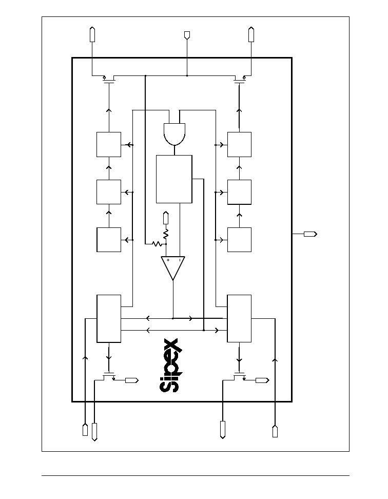
Figure 1. Internal Block Diagram for the SP2526
M4
M3
M1
M2
ENA
FLAGA
GND
OUTA
GND
FLAGB
OUTB
GND
ENB
V
REF
UVLO
OVER TEMPERATURE
SHUT DOWN B
SHUT DOWN A
COMPARATOR
VOLTAGE
REFERENCE
AND
TEMPERATURE
SENSING
FOLDBACK B
FOLDBACK A
CHARGE PUMP B
CHARGE PUMP A
OSCILLATOR B
OSCILLATOR A
LOGIC B
LOGIC A
GND
IN
1
2
3
4
6
6
6
6
8
7
5
SP2526
6
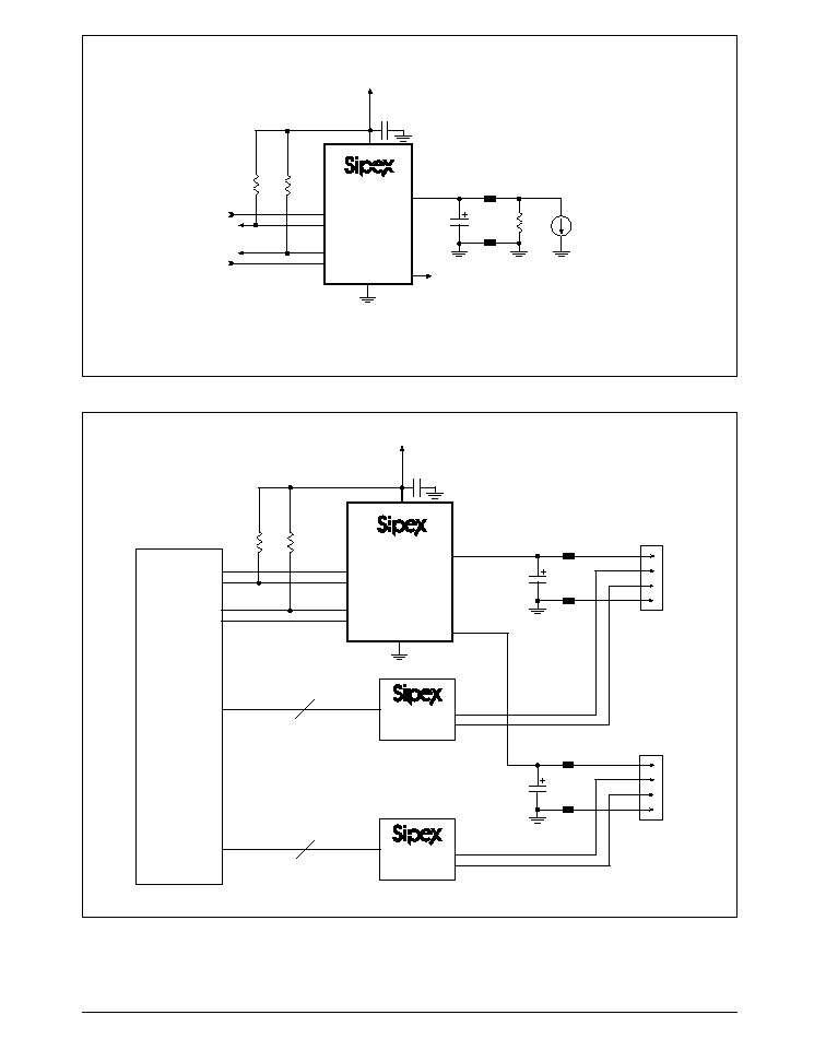
Rev. 8/21/01 SP2526 +3.0V to +5.5V USB Power Control Switch © Copyright 2001 Sipex Corporation
Figure 2. Test Circuit for the SP2526
Figure 3. Typical Application Circuit for the SP2526
6 GND
SP2526
1 ENA
2 FLGA
3 FLGB
4 ENB
8
IN
5
100k
V
IN
C
L
R
L
I
LOAD
*
Ferrite
Bead
Ferrite
Bead
100k
7
OUTA
OUTB
0.1
µ
F
*For current limit response characteristics
6 GND
SP2526
1 ENA
2 FLGA
3 FLGB
4 ENB
8
7
IN
5
100k
C
L
Ferrite
Bead
Ferrite
Bead
100k
V
BUS
D+
D-
GND
D+
D-
SP5301
C
L
Ferrite
Bead
Ferrite
Bead
V
BUS
D+
D-
GND
D+
D-
SP5301
USB
Controller
USB
Port 1
USB
Port 2
OUTA
OUTB
V
IN
0.1
µ
F

7
Rev. 8/21/01 SP2526 +3.0V to +5.5V USB Power Control Switch © Copyright 2001 Sipex Corporation
minimum current of 0.5A to be delivered.
The SP2526 MOSFET switches will exhibit
very low resistance (<100m
) or voltage drop
until the current limit is reached. The fold back
current is the current that is delivered into a short
circuit at the output.
If the SP2526 MOSFET switch is enabled into a
heavy load or short-circuit, the switch will im-
mediately go into a constant-current mode, re-
ducing the output voltage. The respective fault
flag will pull low until the condition is removed.
When a heavy load is connected to the SP2526
switch output, a large transient current may flow
until the current limiting circuitry responds.
The SP2526 will provide a low resistance switch
(100m
) between the input and output pins.
This low resistance will be maintained with
increasing current until the 2.2A limit is reached.
If load current exceeds this limit, the switch will
increase its resistance. The foldback current
(500mA minimum) is reached when there is a
short applied to the output. The 100m
switch
resistance is guaranteed for all load currents,
increasing or decreasing, that are below 500mA.
Thermal Shutdown
Under nominal load conditions, the switch resis-
tance is very low and internal power dissipation
is low. Under short circuit conditions, current is
limited and internal power dissipation is higher
but not extreme. Under intermediate load condi-
tions, both the voltage across the switch and the
current through the switch are at intermediate
values and internal power dissipation is highest.
In this last condition, the die temperature will
reach the thermal limit and the switches in both
channels will be shut off. As the die subse-
quently cools, the switch will turn on again. If
the load is not removed, the device will thermal
cycle in this manner to protect itself from dam-
age.
Thermal shutdown is asserted if the die tempera-
ture exceeds 135
O
C and will not release until the
die termperature drops below 125
O
C. Thermal
shutdown will disable both output MOSFET
switches and force both FLGA and FLGB fault
flags low.
The delay between a current limit fault and
thermal shutdown will vary with ambient tem-
perature, board layout, and load impedance, but
is typically several hundred milliseconds. A
designer
can command a USB controller to recognize the
fault and disable the appropriate channel within
this time.
TYPICAL APPLICATIONS
Bypass Capacitors
A 0.1
µ
F to 1.0
µ
F bypass capacitor from the IN
pin to the GND pin is recommended to control
power supply transients. Refer to Figure 4.
Without a bypass capacitor, an output short may
cause sufficient ringing and damage the device.
Without a bypass capacitor, excessive supply
lead inductance is also a concern.
Input or output transients must not exceed the
absolute maximum supply voltage of V
IN(MAX)
=
+6.0V even for a short duration to avoid risk of
damage to the device.
Transient Overcurrent Filter
When the SP2526 is enabled, large values of
capacitance at the output of the device will cause
inrush current to exceed the short circuit current-
limit threshold of the device and assert a flag
fault condition for FLGA and/or FLGB. The
duration of this time will depend on the size of
the output capacitance. During the capacitance
charging time, the device enters into foldback
mode. As the capacitance is charged, the current
decreases below the current-limit threshold and
the fault flags that are present at the FLGA and/
or FLGB pins will then be deasserted.
In USB applications, it is required that output
bulk capacitance is utilized to support hot-plug
occurences. When the SP2526 is enabled, the
flag may go active for about 1ms due to inrush
current exceeding the current-limit setpoint.
Additionally, during hot-plug events, inrush cur-
rents may also cause the fault flags at the FLGA
and/or FLGB pins to go active. Since these
conditions are not valid overcurrent faults, the
USB controller must ignore the fault flags during
these events. To prevent this, a 1ms RC filter can
be implemented as shown in Figure 5. Alterna-

8
Rev. 8/21/01 SP2526 +3.0V to +5.5V USB Power Control Switch © Copyright 2001 Sipex Corporation
tively, a 1ms debounce routine may be pro-
grammed into the USB logic controller, elimi-
nating the need for the RC filter.
Soft Start Condition
The soft start feature of the SP2526 is imple-
mented by holding the output turn-on rise time
to 1ms. When off, the device has high imped-
ance MOSFET channels that slowly become
low impedance as the device powers on. This
prevents an inrush current from causing voltage
drops that result from charging a capacitive
load and can pull the USB voltage bus below
specified levels. This satisfies the USB voltage
droop requirements for bus-powered applica-
tions. Refer to the circuit in Figure 6.
The SP2526 can provide inrush current limiting
for applications with large load capacitances
where C
BULK
> 10
µ
F. Refer to the circuit in
Figure 7 for a configuration that will meet USB
transient regulation specifications with large
load capacitances.
Enable Input
The ENA and ENB control pins must be driven
to a logic high or logic low for a clearly defined
signal input. Floating these control lines may
cause unpredictable operation.
USB Compliance
The SP2526 is ideal for self-powered and bus-
powered Universal Serial Bus (USB) applica-
tions. A USB port provides a +5.0V bus and
ground return line in addition to a twisted pair
for data.
The SP2526 will comply with the following
USB requirements:
1) The fault current is well below the UL 25VA
safety requirements;
2) The Flag Outputs are available to indicate
fault conditions to USB controllers;
3) The MOSFET switches' low on-resistance
meets USB voltage drop requirements;
4) Each MOSFET switch channel can supply
500mA as required by USB downstream devices;
5) Soft start eliminates any momentary voltage
drops on the upstream port that may occur when
the switches are enabled in bus-powered applica-
tions.
Refer to Table 1 for a USB compliance summary
of the SP2526. Additional features include the
following:
6) An Undervoltage Lockout ensures that the
device remains off unless there is a valid input
supply voltage present;
7) +3.3V and +5.0V logic compatible enable
inputs;
8) Thermal Shutdown prevents the possiblity of
catastrophic switch failure from high-current
loads;
8) The device is available in both active-high and
active-low versions.
Refer to Figures 8 to 26 for typical performance
characteristics of the SP2526.

9
Rev. 8/21/01 SP2526 +3.0V to +5.5V USB Power Control Switch © Copyright 2001 Sipex Corporation
Figure 5. An RC Filter for Overcurrent Faults
Figure 4. Bypass Capacitor at the Supply Pins
Table 1. USB Protocol Compliance of the SP2526 device
t
n
e
m
e
r
i
u
q
e
R
B
S
U
e
r
u
t
a
e
F
t
n
a
i
l
p
m
o
C
6
2
5
2
P
S
d
e
r
i
u
q
e
r
g
n
i
t
i
m
il
t
n
e
r
r
u
c
h
s
u
r
n
I
s
m
1
n
i
n
o
s
n
r
u
t
t
r
a
t
s
t
f
o
S
0
0
5
<
f
o
e
t
a
t
S
d
n
e
p
s
u
S
µ
d
e
r
i
u
q
e
R
A
1
f
o
t
n
e
r
r
u
C
d
n
e
p
s
u
S
µ
m
u
m
i
x
a
m
A
m
u
m
i
x
a
m
V
m
0
5
3
e
v
a
h
t
s
u
m
s
b
u
h
d
e
r
e
w
o
p
s
u
B
t
r
o
p
o
t
g
u
l
p
e
l
b
a
c
m
o
r
f
p
o
r
d
m
0
4
1
f
o
e
c
n
a
t
s
i
s
e
r
n
o
h
c
t
i
w
S
m
u
m
i
x
a
m
)
A
m
0
0
5
t
a
V
m
0
7
o
t
s
e
t
a
l
s
n
a
r
t
(
V
5
2
.
5
+
o
t
V
5
7
.
4
+
s
i
t
r
o
p
b
u
h
r
o
t
s
o
h
o
t
d
e
il
p
p
u
s
e
g
a
t
l
o
V
V
5
.
5
+
o
t
V
0
.
3
+
f
o
e
g
n
a
r
g
n
i
t
a
r
e
p
O
e
l
b
a
t
s
a
e
v
a
h
t
s
u
m
r
e
w
o
p
s
u
b
s
w
a
r
d
t
a
h
t
e
c
i
v
e
d
A
V
f
o
s
m
0
0
1
n
i
h
t
i
w
y
l
p
p
u
s
S
U
B
V
4
.
4
+
g
n
i
h
c
a
e
r
s
m
1
n
i
n
o
s
n
r
u
T
d
e
r
i
u
q
e
r
y
t
il
i
b
a
p
a
c
g
n
i
t
r
o
p
e
r
t
n
e
r
r
u
c
-
r
e
v
O
s
g
a
l
f
t
l
u
a
f
n
i
a
r
d
n
e
p
O
ENA 1
FLGA 2
FLGB 3
ENB 4
0.1
µ
F to 1.0
µ
F
8 OUTA
7 IN
6 GND
5 OUTB
SP2526
V
IN
ENA 1
FLGA 2
FLGB 3
ENB 4
USB
Controller
0.1
µ
F
8 OUTA
7 IN
6 GND
5 OUTB
SP2526
OVERCURRENT
10k
10k
V
IN
10
Rev. 8/21/01 SP2526 +3.0V to +5.5V USB Power Control Switch © Copyright 2001 Sipex Corporation
ENA 1
FLGA 2
FLGB 3
ENB 4
USB
Controller
USB
Cable
4.7
µ
F
8 OUTA
7 IN
6 GND
5 OUTB
0.1
µ
F
SP2526
C
BULK
USB
Cable
Downstream
USB Device
USB Powered Hub
USB Host
V
BUS
GND
Figure 6. Soft Start Circuit Configuration for a Single Channel USB-powered Application with the SP2526
Figure 7. Soft Start Circuit Configuration for SP2526 Applications with Large Load Capacitances
ENA 1
FLGA 2
FLGB 3
ENB 4
USB
Controller
4.7
µ
F
8 OUTA
7 IN
6 GND
5 OUTB
0.1
µ
F
SP2526-2
C
BULK
USB
Cable
USB Peripheral
USB Host
V
BUS
GND
C
BULK
OUTA
OUTB
GND
GND
PORT A
PORT B
11
Rev. 8/21/01 SP2526 +3.0V to +5.5V USB Power Control Switch © Copyright 2001 Sipex Corporation
Figure 8. Output On-Resistance vs. Supply Voltage
Figure 9. Output On-Resistance vs. Temperature
Figure 10. Undervoltage Threshold Voltage vs.
Temperature
Figure 11. Control Threshold vs. Supply Voltage
PERFORMANCE CHARACTERISTICS
V
IN
= +5.0V, single MOSFET switch section, and T
AMB
= +25
O
C unless otherwise noted.
On-Resistance (millohms)
Output-On-Resistance (millohms)
UVLO Threshold Voltage (V)
Enable Threshold Voltage (V)
Output On-Resistance vs. Supply Voltage
80
84
88
92
96
100
2.5
3
3.5
4
4.5
5
5.5
6
Supply Voltage (V)
Output On-Resistance vs. Temperature
60
70
80
90
100
110
120
-40
-20
0
20
40
60
80
100
Temperature (∞C)
Vcc=5V
UVLO Threshold Voltage
vs. Temperature
2.68
2.7
2.72
2.74
2.76
2.78
2.8
2.82
2.84
2.86
2.88
-40
-20
0
20
40
60
80
100
Temperature (∞C)
Rising
Falling
Enable Threshold Voltage vs. Supply Voltage
0.9
1.1
1.3
1.5
1.7
1.9
2.1
2.3
2.5
3
3.5
4
4.5
5
Supply Voltage (V)
Enable Voltage Rising
Enable Voltage Falling

12
Rev. 8/21/01 SP2526 +3.0V to +5.5V USB Power Control Switch © Copyright 2001 Sipex Corporation
Figure 12. On-state Supply Current vs. Supply Voltage
Figure 13. Off-state Supply Current vs. Supply Voltage
Figure 14. On-state Supply Current vs. Temperature
Figure 15. Off-state Supply Current vs. Temperature
PERFORMANCE CHARACTERISTICS (continued)
V
IN
= +5.0V, single MOSFET switch section, and T
AMB
= +25
O
C unless otherwise noted.
Supply Current (
µ
A)
Offstate Supply Current (
µ
A)
Supply Current (
µ
A)
Offstate Supply Current (
µ
A)
Supply Current vs. Supply Voltage
60
70
80
90
100
110
120
3
3.5
4
4.5
5
5.5
Supply Voltage (V)
Offstate Supply Current
vs. Supply Voltage
0.0
0.2
0.4
0.6
0.8
1.0
1.2
1.4
1.6
1.8
3
3.5
4
4.5
5
5.5
Supply Voltage (V)
Supply Current vs. Temperature
75
80
85
90
95
100
-40
-20
0
20
40
60
80
100
Temperature (∞C)
Vcc=5V
Switches Enabled
Offstate Supply Current
vs. Temperature
0.0
0.5
1.0
1.5
2.0
2.5
3.0
3.5
4.0
4.5
5.0
-40
-20
0
20
40
60
80
100
Temperature (∞C)
Vcc=5V
Switches Disabled
13
Rev. 8/21/01 SP2526 +3.0V to +5.5V USB Power Control Switch © Copyright 2001 Sipex Corporation
Figure 16. Control Threshold vs. Temperature
Figure 17. Input Voltage Response
Figure 18. Current-Limit Response With a Ramped
Load
Figure 19. Turn-on/Turn-off Characteristics Where
R
L
= 35
and C
L
= 10
µ
F
PERFORMANCE CHARACTERISTICS (continued)
V
IN
= +5.0V, single MOSFET switch section, and T
AMB
= +25
O
C unless otherwise noted.
V
IN
V
OUT
I
OUT
FLAG
200mA/Div
SP2526 Rev B
Enable Threshold Voltage (V)
C
L
= 10
µ
F
R
L
= 35
FLAG
V
OUT
I
OUT
I
OUT
V
OUT
FLAG
EN
R
L
35
C
L
= 10
µ
F
Enable Threshold Voltage
vs. Temperature
1.5
1.7
1.9
2.1
2.3
2.5
-40
-20
0
20
40
60
80
100
Temperature (∞C)
Vcc=5V
Enable Voltage Rising
Enable Voltage Falling
14
Rev. 8/21/01 SP2526 +3.0V to +5.5V USB Power Control Switch © Copyright 2001 Sipex Corporation
Figure 20. Turn-on/Turn-off Characteristics where R
L
=
35
and C
L
= 150
µ
F
Figure 21. Short Circuit Response (Enable into Short
Circuit)
Figure 22. Short Circuit Response (Short Applied To
Output)
Figure 23. Short Circuit Transient Response (Short
Applied To Output)
PERFORMANCE CHARACTERISTICS (continued)
V
IN
= +5.0V, single MOSFET switch section, and T
AMB
= +25
O
C unless otherwise noted.
200mA/ Div
R
L
= 35
C
L
= 150
µ
F
SP2526 Rev B
EN
FLAG
V
OUT
I
OUT
EN
FLAG
I
OUT
V
OUT
0.5A/DIV
SP2526 Rev B
I
OUT
V
OUT
FLAG
1A/DIV
2A/DIV
I
OUT
V
OUT
FLAG
SP2526 Rev B
15
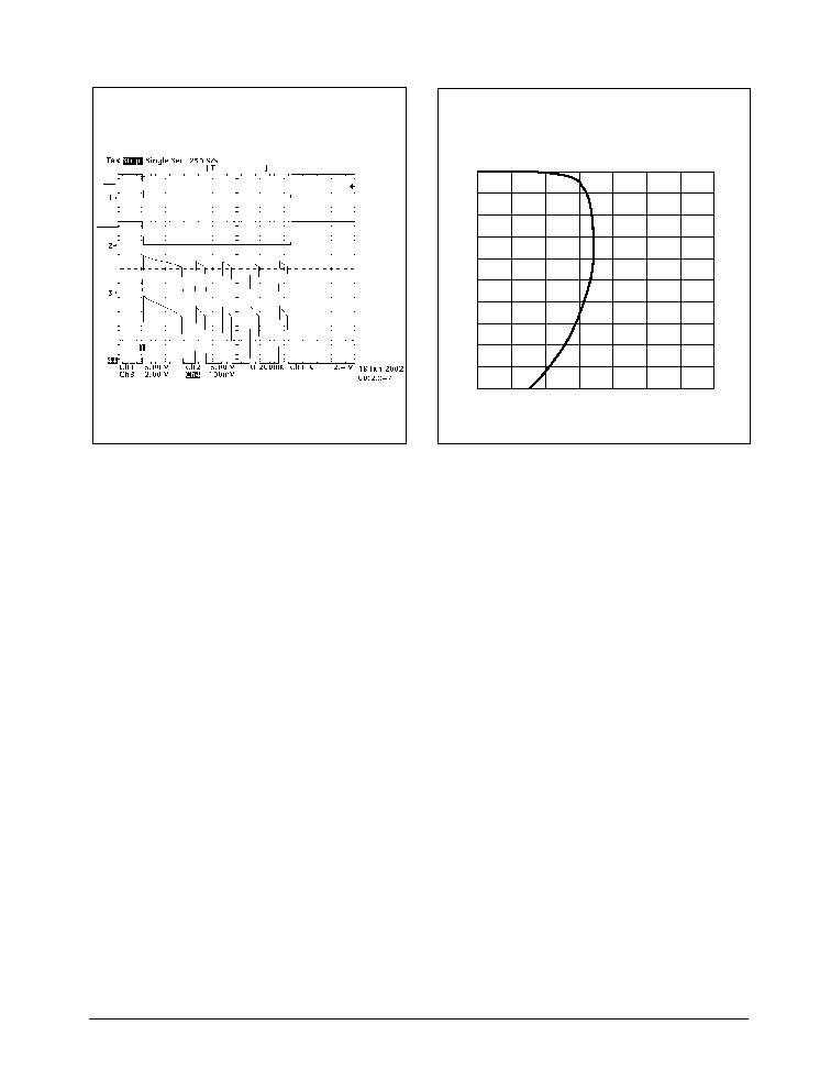
Rev. 8/21/01 SP2526 +3.0V to +5.5V USB Power Control Switch © Copyright 2001 Sipex Corporation
Figure 24. Short Circuit Response (Enable into Short
Circuit)
Figure 25. Current Limit Response (Pulsed Load
applied at Output)
PERFORMANCE CHARACTERISTICS (continued)
V
IN
= +5.0V, single MOSFET switch section, and T
AMB
= +25
O
C unless otherwise noted.
EN
FLAG
I
OUT
V
OUT
1A/DIV
SP2526 Rev B
R
L
= 1
0
0.5
1
1.5
2
2.5
3
3.5
4
4.5
5
0
0.5
1
1.5
2
2.5
3
3.5
I
OUT
V
OUT
V
IN
= 5
16
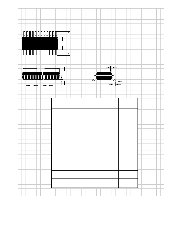
Rev. 8/21/01 SP2526 +3.0V to +5.5V USB Power Control Switch © Copyright 2001 Sipex Corporation
D
E
H
PACKAGE: PLASTIC
SMALL OUTLINE (SOIC)
(NARROW)
DIMENSIONS (Inches)
Minimum/Maximum
(mm)
8≠PIN
A
A1
ÿ
L
B
e
h x 45
∞
A
A1
B
D
E
e
H
h
L
ÿ
0.053/0.069
(1.346/1.748)
0.004/0.010
(0.102/0.249
0.014/0.019
(0.35/0.49)
0.189/0.197
(4.80/5.00)
0.150/0.157
(3.802/3.988)
0.050 BSC
(1.270 BSC)
0.228/0.244
(5.801/6.198)
0.010/0.020
(0.254/0.498)
0.016/0.050
(0.406/1.270)
0
∞
/8
∞
(0
∞
/8
∞
)
14≠PIN
0.053/0.069
(1.346/1.748)
0.004/0.010
(0.102/0.249)
0.013/0.020
(0.330/0.508)
0.337/0.344
(8.552/8.748)
0.150/0.157
(3.802/3.988)
0.050 BSC
(1.270 BSC)
0.228/0.244
(5.801/6.198)
0.010/0.020
(0.254/0.498)
0.016/0.050
(0.406/1.270)
0
∞
/8
∞
(0
∞
/8
∞
)
16≠PIN
0.053/0.069
(1.346/1.748)
0.004/0.010
(0.102/0.249)
0.013/0.020
(0.330/0.508)
0.386/0.394
(9.802/10.000)
0.150/0.157
(3.802/3.988)
0.050 BSC
(1.270 BSC)
0.228/0.244
(5.801/6.198)
0.010/0.020
(0.254/0.498)
0.016/0.050
(0.406/1.270)
0
∞
/8
∞
(0
∞
/8
∞
)
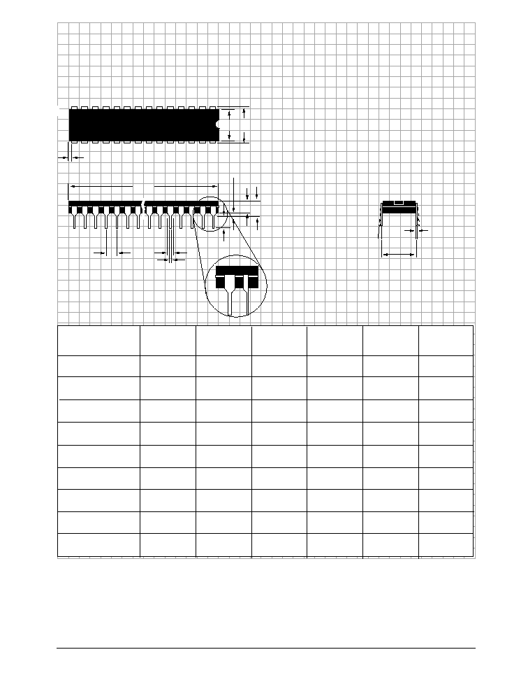
17
Rev. 8/21/01 SP2526 +3.0V to +5.5V USB Power Control Switch © Copyright 2001 Sipex Corporation
D
ALTERNATE
END PINS
(BOTH ENDS)
D1 = 0.005" min.
(0.127 min.)
E
PACKAGE: PLASTIC
DUAL≠IN≠LINE
(NARROW)
DIMENSIONS (Inches)
Minimum/Maximum
(mm)
A = 0.210" max.
(5.334 max).
E1
C
ÿ
L
A2
A1 = 0.015" min.
(0.381min.)
B
B1
e = 0.100 BSC
(2.540 BSC)
e
A
= 0.300 BSC
(7.620 BSC)
A2
B
B1
C
D
E
E1
L
ÿ
8≠PIN
0.115/0.195
(2.921/4.953)
0.014/0.022
(0.356/0.559)
0.045/0.070
(1.143/1.778)
0.008/0.014
(0.203/0.356)
0.355/0.325
(9.017/10.160)
0.300/0.325
(7.620/8.255)
0.240/0.280
(6.096/7.112)
0.115/0.150
(2.921/3.810)
0
∞
/ 15
∞
(0
∞
/15
∞
)
14≠PIN
0.115/0.195
(2.921/4.953)
0.014/0.022
(0.356/0.559)
0.045/0.070
(1.143/1.778)
0.008/0.014
(0.203/0.356)
0.735/0.775
(18.669/19.685)
0.300/0.325
(7.620/8.255)
0.240/0.280
(6.096/7.112)
0.115/0.150
(2.921/3.810)
0
∞
/ 15
∞
(0
∞
/15
∞
)
0.115/0.195
(2.921/4.953)
0.014/0.022
(0.356/0.559)
0.045/0.070
(1.143/1.778)
0.008/0.014
(0.203/0.356)
0.780/0.800
(19.812/20.320)
0.300/0.325
(7.620/8.255)
0.240/0.280
(6.096/7.112)
0.115/0.150
(2.921/3.810)
0
∞
/ 15
∞
(0
∞
/15
∞
)
16≠PIN
18≠PIN
0.115/0.195
(2.921/4.953)
0.014/0.022
(0.356/0.559)
0.045/0.070
(1.143/1.778)
0.008/0.014
(0.203/0.356)
0.880/0.920
(22.352/23.368)
0.300/0.325
(7.620/8.255)
0.240/0.280
(6.096/7.112)
0.115/0.150
(2.921/3.810)
0
∞
/ 15
∞
(0
∞
/15
∞
)
20≠PIN
0.115/0.195
(2.921/4.953)
0.014/0.022
(0.356/0.559)
0.045/0.070
(1.143/1.778)
0.008/0.014
(0.203/0.356)
0.980/1.060
(24.892/26.924)
0.300/0.325
(7.620/8.255)
0.240/0.280
(6.096/7.112)
0.115/0.150
(2.921/3.810)
0
∞
/ 15
∞
(0
∞
/15
∞
)
0.115/0.195
(2.921/4.953)
0.014/0.022
(0.356/0.559)
0.045/0.070
(1.143/1.778)
0.008/0.014
(0.203/0.356)
1.145/1.155
(29.083/29.337)
0.300/0.325
(7.620/8.255)
0.240/0.280
(6.096/7.112)
0.115/0.150
(2.921/3.810)
0
∞
/ 15
∞
(0
∞
/15
∞
)
22≠PIN
18
Rev. 8/21/01 SP2526 +3.0V to +5.5V USB Power Control Switch © Copyright 2001 Sipex Corporation
Model
Temperature Range
Package Types
SP2526-1EN ................................................... -40
∞
C to +85
∞
C ................................................... 8-pin NSOIC
SP2526-1EN/TR .............................................. -40
∞
C to +85
∞
C ........................... (Tape & Reel) 8-pin NSOIC
SP2526-2EN ................................................... -40
∞
C to +85
∞
C ................................................... 8-pin NSOIC
SP2526-2EN/TR .............................................. -40
∞
C to +85
∞
C ........................... (Tape & Reel) 8-pin NSOIC
ORDERING INFORMATION
Corporation
SIGNAL PROCESSING EXCELLENCE
Sipex Corporation reserves the right to make changes to any products described herein. Sipex does not assume any liability arising out of the
application or use of any product or circuit described hereing; neither does it convey any license under its patent rights nor the rights of others.
Sipex Corporation
Headquarters and
Sales Office
22 Linnell Circle
Billerica, MA 01821
TEL: (978) 667-8700
FAX: (978) 670-9001
e-mail: sales@sipex.com